
For millennia, glass has been the hallmark of human craftsmanship, evolving from primitive obsidian tools to the sophisticated fiber optics that underpin the modern internet. Today, this ancient material is undergoing a high-tech metamorphosis that places it at the very center of the artificial intelligence revolution. As the world’s most powerful data centers struggle to keep pace with the voracious computational demands of generative AI, the semiconductor industry is looking beyond traditional silicon and plastic. The emergence of glass substrates represents a fundamental shift in how computing hardware is designed, manufactured, and cooled, promising a new era of energy efficiency and processing density.
The move toward glass is driven by a looming "mechanical wall" in semiconductor packaging. For decades, the industry has relied on organic substrates—typically a composite of fiberglass-reinforced epoxy—to serve as the foundation upon which silicon chips are mounted. This substrate acts as the interface between the microscopic circuitry of the chip and the macroscopic world of the circuit board. However, as AI workloads grow in complexity, the chips themselves are becoming larger and hotter. This creates a physical crisis: the organic materials used in current packaging possess a different thermal expansion coefficient than the silicon chips they support. When these high-performance chips reach peak operating temperatures, the resulting heat causes the organic substrate to warp and distort.
This phenomenon, known in the industry as warpage, is more than a mere nuisance. As Deepak Kulkarni, a senior fellow at Advanced Micro Devices (AMD), notes, these mechanical constraints are beginning to dictate the very trajectory of high-performance computing. When a substrate warps, the delicate electrical connections between components can misalign or break, leading to chip failure or significant throttles in performance. Furthermore, uneven surfaces prevent efficient cooling, creating a vicious cycle where heat leads to distortion, which in turn leads to even more heat. Glass, with its exceptional thermal stability and rigidity, offers a way out of this structural dead end.
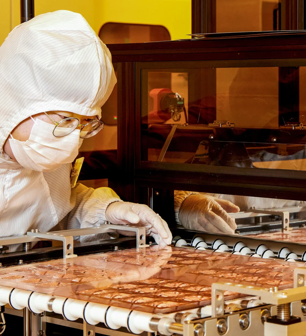
The transition is already moving from the laboratory to the factory floor. Absolics, a subsidiary of the South Korean materials giant SKC, is currently at the vanguard of this commercialization effort. The company recently completed a specialized manufacturing facility in Covington, Georgia, dedicated entirely to the production of glass substrates. This facility is expected to begin commercial manufacturing within the current year, marking a significant milestone in the domestic U.S. semiconductor supply chain. The project has garnered substantial institutional support, including $175 million in grants from the U.S. government’s CHIPS for America program, signaling that glass technology is now viewed as a matter of national strategic importance.

The advantages of glass extend far beyond its resistance to heat. One of the most critical metrics in modern chip design is interconnect density—the number of electrical pathways that can be squeezed into a given area. Because glass is incredibly flat and dimensionally stable, engineers can drill much finer holes, known as Through Glass Vias (TGVs), to create signal and power connections. Rahul Manepalli, vice president of advanced packaging at Intel, suggests that glass could allow for a tenfold increase in connection density compared to organic materials. This density allows designers to pack 50% more silicon into the same physical footprint, effectively extending the lifespan of Moore’s Law through clever packaging rather than just shrinking transistors.
Furthermore, the surface of glass is remarkably smooth—up to 5,000 times smoother than traditional organic substrates. In the world of semiconductor fabrication, where even a microscopic speck of dust can ruin a multi-thousand-dollar wafer, this level of smoothness is transformative. It eliminates the tiny surface defects that often lead to "shorts" or signal degradation when metal layers are deposited onto the substrate. By reducing these defects, manufacturers can improve their yields, eventually lowering the cost of high-end AI hardware once the technology scales.
While the immediate focus is on massive data centers and AI training clusters, the long-term implications for consumer electronics are profound. As production processes mature and costs inevitably decline, the benefits of glass-core substrates—better battery life due to energy efficiency and thinner device profiles due to increased chip density—will likely trickle down to premium laptops and smartphones. We are seeing the beginning of a broader industrial race, with heavyweights like Samsung Electronics, Samsung Electro-Mechanics, and LG Innotek all accelerating their glass packaging research. This is no longer an experimental niche; it is a full-scale pivot by the world’s leading electronics manufacturers.
The shift is also creating a new ecosystem of specialized suppliers. Companies like JNTC, which traditionally focused on tempered glass for mobile displays, are now retooling their facilities to produce semi-finished glass panels for the semiconductor industry. These panels come pre-drilled and coated with thin metal layers, ready to be integrated into complex chip packages. By 2025, the market for glass in semiconductors is projected to be worth $1 billion, with analysts at IDTechEx forecasting a surge to $4.4 billion by 2036. This growth reflects a growing consensus that the "organic era" of chip packaging is reaching its twilight.
Perhaps the most futuristic application of glass substrates lies in the field of silicon photonics. Unlike organic materials, glass is transparent and can be engineered to guide light. This opens the door to integrating optical interconnects directly into the substrate. Currently, chips communicate using copper wires, which generate significant heat and consume vast amounts of power as data transfer speeds increase. Replacing these "power-hungry" copper pathways with light-based signals would revolutionize energy efficiency. A glass-based system could move data across a chip package with a fraction of the energy required by today’s hardware, addressing one of the most significant bottlenecks in AI scaling: the sheer cost of electricity.

However, the road to a glass-based future is not without its obstacles. The very property that makes glass desirable—its rigidity—also makes it brittle. In the early stages of research, manufacturing glass panels that were only 700 micrometers thick resulted in frequent breakage. Intel’s development teams famously struggled with hundreds of cracked panels during early testing phases. Overcoming this fragility required years of materials science research, leading to the development of specialized handling tools and protective coatings that allow glass to survive the rigorous stresses of a semiconductor assembly line. In early 2025, Intel reached a symbolic breakthrough by successfully booting the Windows operating system on a functional device powered by a glass-core substrate, proving that the technology is ready for real-world applications.
The geographical distribution of this technology is also noteworthy. While much of the foundational research began at institutions like the Georgia Institute of Technology, the commercial race is spanning the globe. South Korean firms are leveraging their expertise in display glass to gain an early lead, while Chinese manufacturers are rapidly investing in the supply chain to ensure they aren’t left behind in the AI hardware race. The involvement of the U.S. CHIPS Act highlights a desire to keep this critical manufacturing capability onshore, particularly as it relates to the high-performance computing (HPC) sector.
As we look toward the end of the decade, the integration of glass into the heart of our computing infrastructure seems inevitable. The surge in AI workloads has acted as a catalyst, forcing the industry to solve mechanical and thermal problems that were once considered distant concerns. By providing a platform that is smoother, flatter, and more thermally resilient than anything that came before, glass is enabling a new generation of "chiplet" designs. These designs, which combine multiple specialized chips into a single powerful system, represent the future of high-performance silicon.
In conclusion, the transition to glass substrates is more than a simple material swap; it is a foundational upgrade to the architecture of the digital age. By solving the persistent problem of thermal warpage and unlocking the potential for optical data transfer, glass is providing the "mighty" foundation required for the next leap in artificial intelligence. What was once a fragile material used for windows and art has become the bedrock of the most complex machines ever built, ensuring that the trajectory of human innovation remains unburdened by the physical limits of the past. As the first commercial glass-backed chips begin to roll off production lines this year, the industry is not just looking through a glass darkly—it is seeing a clearer, faster, and more efficient path forward for the entire world of technology.
